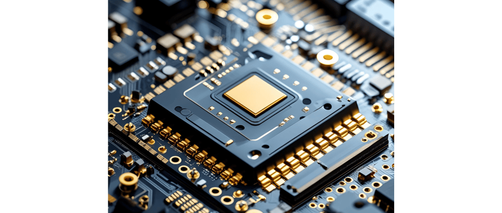
Integrated Circuit Package Types
Integrated circuits are manufactured in various package types that determine their physical form factor, mounting method, and electrical connections.
INTEGRATED CIRCUIT
8/19/20253 min read
Integrated Circuit Package Types: DIP and SMD Classifications
Integrated circuits are manufactured in various package types that determine their physical form factor, mounting method, and electrical connections. The two primary classifications for integrated circuit packages are Dual In-line Package (DIP) and Surface Mount Device (SMD), each offering distinct advantages for different application requirements and manufacturing processes.
Dual In-line Package (DIP) Types
Dual In-line Package integrated circuits represent the traditional through-hole mounting technology that dominated electronic manufacturing for decades. DIP packages feature two parallel rows of pins extending from opposite sides of a rectangular plastic or ceramic body. These pins are designed to pass through holes drilled in printed circuit boards and are secured through wave soldering or selective soldering processes.
Standard DIP packages are available in various configurations, typically designated by their pin count and spacing. Common DIP formats include 8-pin, 14-pin, 16-pin, 18-pin, 20-pin, 24-pin, 28-pin, and 40-pin configurations, with standard pin spacing of 0.1 inches (2.54 millimeters) between adjacent pins. The package width varies according to the pin count, with narrow DIP packages measuring 0.3 inches (7.62 millimeters) wide and wide DIP packages measuring 0.6 inches (15.24 millimeters) across.
Ceramic DIP packages provide enhanced thermal performance and superior environmental protection compared to plastic alternatives. These packages utilize ceramic materials that offer excellent heat dissipation properties and resistance to temperature extremes, making them suitable for military, aerospace, and high-reliability applications where operating conditions may exceed standard commercial specifications.
Plastic DIP packages represent the most cost-effective solution for commercial applications. These packages utilize molded plastic bodies that provide adequate protection for integrated circuits operating in standard commercial environments while maintaining low manufacturing costs suitable for high-volume production.
Surface Mount Device (SMD) Types
Surface Mount Device packages enable high-density circuit board layouts through their compact form factors and surface-mounting methodology. SMD packages are soldered directly to pads on the circuit board surface rather than passing through holes, allowing for smaller component sizes and higher component density per unit area.
Small Outline Integrated Circuit packages, commonly abbreviated as SOIC, feature gull-wing leads extending from two sides of a rectangular package body. SOIC packages provide significant space savings compared to equivalent DIP packages while maintaining reasonable ease of handling and rework capabilities. Standard SOIC packages are available in narrow and wide body configurations with pin counts ranging from 8 to 32 pins.
Thin Small Outline Package configurations, designated as TSOP, offer reduced package thickness for applications requiring minimal profile heights. TSOP packages typically feature leads extending from two or four sides of the package body and are commonly used for memory devices and high pin-count applications where space constraints are critical.
Quad Flat Package types, known as QFP, position leads on all four sides of square or rectangular package bodies. QFP packages accommodate high pin counts while maintaining manageable package sizes suitable for complex integrated circuits such as microprocessors and application-specific circuits. Pin counts for QFP packages commonly range from 32 to 256 pins with various pitch options available.
Ball Grid Array packages, abbreviated as BGA, utilize an array of solder balls positioned on the bottom surface of the package rather than traditional leads. BGA packages enable extremely high pin counts and superior electrical performance through shorter connection paths and reduced parasitic effects. These packages are particularly suitable for high-performance processors and complex system-on-chip implementations.
Chip Scale Package solutions, designated as CSP, provide the smallest possible package sizes by minimizing the package overhead relative to the integrated circuit die size. CSP packages typically measure only slightly larger than the actual semiconductor die, enabling maximum space efficiency in compact electronic designs.
Package Selection Considerations
The selection between DIP and SMD package types depends on several critical factors including manufacturing requirements, space constraints, performance specifications, and cost considerations. DIP packages offer advantages in prototyping environments, educational applications, and situations requiring easy component replacement or circuit modification. The through-hole mounting method provides robust mechanical connections that can withstand significant mechanical stress and thermal cycling.
SMD packages provide superior performance characteristics through reduced parasitic inductance and capacitance, enabling higher operating frequencies and improved signal integrity. The compact form factors enable higher circuit density and reduced board space requirements, making SMD packages essential for portable electronics and space-constrained applications.
Manufacturing considerations also influence package selection decisions. DIP packages require drilling operations and specialized through-hole assembly equipment, while SMD packages utilize surface mount assembly processes that enable automated high-volume manufacturing with superior consistency and reliability.
Thermal management capabilities vary significantly between package types, with SMD packages generally providing superior heat dissipation through their direct connection to the circuit board thermal plane. However, certain ceramic DIP packages offer exceptional thermal performance for high-power applications requiring maximum heat dissipation capabilities.
Cost factors encompass both component pricing and assembly expenses. While SMD packages typically offer lower per-unit costs for high-volume applications, DIP packages may provide cost advantages for low-volume or prototype applications where specialized assembly equipment investments cannot be justified.
Understanding these package classifications enables informed selection decisions that optimize performance, cost, and manufacturing efficiency for specific integrated circuit applications across diverse electronic system requirements.
Get in touch
Address
House-132, Modina Mosjid Road, Azampur Kacha Bazar, Uttara, Dhaka
Contacts
01919958219
info@techlarch.com